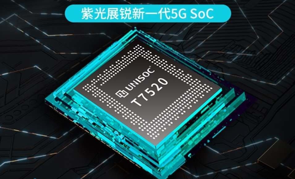
UniSoC T7520 is the first 5G-enabled mobile CPU from Spreadtrum owned UniSoC. And not just that, the SoC also happens to be one of the world’s first chips to be made using TSMC’s 6 nm process, which uses extreme ultraviolet lithography (EUVL) for several layers.
The UNISOC T7520 SoC comes in a big.LITTLE architecture. It has four high-performance ARM Cortex-A76 cores, and other four energy-efficient Arm Cortex-A55 cores. The CPU is bundled with Mali-G57 GPU with a display engine that supports multiple screens. It also support 4K resolution and HDR10+.
Interestingly, the SoC is integrate with a new NPU that is said to offer a 50% higher TOPS-per-Watt rate than the company’s previous-generation NPU. In addition, the chip features a four-core ISP that supports up to 100 MP sensors and multi-camera processing capability.
Finally, the new mobile processor also features the company’s latest Secure Element process that supports ‘most of crypto algorithms’ and can handle compute-intensive security scenarios, such as encrypted video calls etc.
One of the key features of the UNISOC T7520 is of course its integrated 2G/3G/4G/5G-supporting modem, which supports 5G NR TDD+FDD carrier aggregation, as well as uplink and downlink decoupling for enhanced coverage. All told, the T7520’s modem is designed to offer peak uplink speed of 3.25 Gbps.
The high level of integration of the T7520 SoC is designed to enable smartphone manufacturers to build more reasonably priced 5G handsets, which will inevitably increase their popularity and adoption of the technology.
Meanwhile, usage of TSMC’s 6 nm fabrication technology (known as N6) should allow UNISOC to make the Chip for less than compared to non-EUV fabrication processes. We could expect cheaper 5G smartphones once this SoC enter mass production, hopefully before the close of 2020.


